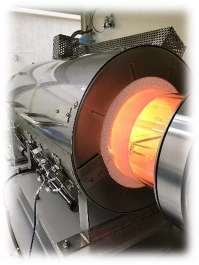
Taiyo Nippon Sanso Corporation (“Nippon Sanso”, President: Kenji Nagata) announces that it has installed its first Ga2O3 MOCVD system in the laboratory of Professor Yoshinao Kumagai at the Tokyo University of Agriculture and Technology.
1. Background
β-gallium oxide (β-Ga2O3) is attracting attention as a semiconductor material for next-generation power (and energy efficient) devices. In October 2020, Nippon Sanso and Tokyo University of Agriculture and Technology started joint research on β-Ga2O3 thin film growth by MOCVD method, and in March 2021, announced the successful MOCVD growth of β-Ga2O3. Nippon Sanso’s newly designed Ga2O3 MOCVD system will make it possible to fabricate complex device structures and further stimulate research and development of these materials.
Nippon Sanso will continue to enhance its Ga2O3 MOCVD technology to enable better energy efficient semiconductor technology to promote its company mission and to support the realization of a carbon-neutral society.
2. Outline of MOCVD system
- Process Capability: 1 × 2-inch wafer
- Model: FR2000-OX
- Features: MOCVD growth chamber for high purity and high-speed growth of oxides on β-Ga2O3 substrates to meet the needs of thick film and alloy growth for research of high performance electronic devices.


